Disclaimer: This tutorial is for simplified demonstration/educational purposes and not intended for production applications. We cannot be held responsible for any misuse, errors, damages, or losses. Use at your own risk. Production implementations of our products follow much more stringent quality control processes that those shown in this tutorial, per our clients’ requirements.
Printed Circuit Boards (PCBs) are ubiquitous – they’re in cell phones, TVs, computers – the list goes on. When companies are developing their medical device, home automation, or even aerospace application, prototyping the concept for customer validation prior to large scale manufacturing, is critical. In this scenario, hand-soldering becomes handy for smaller quantities and for functional validation.
In this tutorial, we’ll show how PCBs can be soldered, principles we hope will help you get validation from your clients, just like how the circuit shown below helped our client obtain critical feedback from his customers. Speed and quality are key in winning in today’s competitive markets.
It’s best to start out with defining our goal, which is to solder all the though-hole and surface mount device (SMD) components for the PCB shown below. The former components penetrate all layers of the board, while the latter only resides on one side of the board.

Our approach will be to solder the SMD devices first. SMD soldering can be accomplished with solder paste, which when heated, will re-flow and solder our components. For this step, it is possible to use a metal cutout, referred to as a stencil, that will apply the solder paste at the SMD pad locations (Step 1A). In this tutorial, we’ll show both; it is possible to get by without a stencil, though not using one usually is a bit messier at the beginning and requires some rework to remove excess solder (Step 1B).

1A. Use Stencil to Apply Solderpaste (Optional)
We can choose to apply solderpaste by using a stencil, which is a metal cutout that aligns with our PCB.

Next, we place the stencil on top of the PCB and align the cutout exactly with the SMD pads. Taping the PCB and the stencil in place is helpful.

Now, we squeeze the solder paste from our syringe and apply it on the stencil.

Additionally, we spread the solder paste with a credit-card-like applier.

Finally, we remove the stencil and reveal the PCB with the applied solder paste.

1B. Apply Solder Paste without Stencil
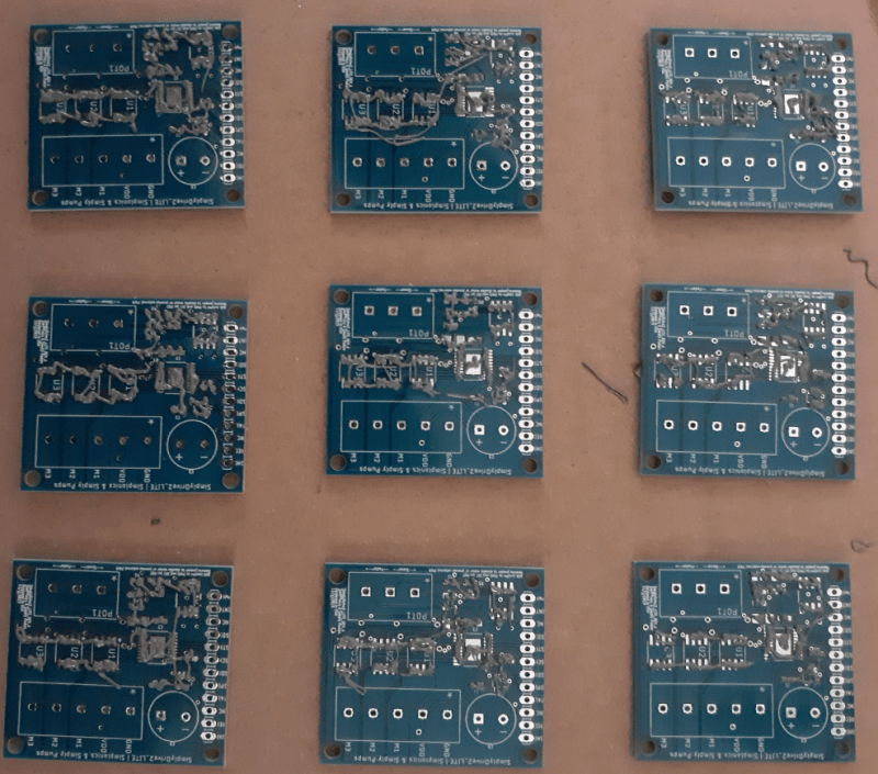
Even without a stencil to cleanly apply solder paste, we’re going to prove that it’s possible to develop a quality circuit. For the purposes of this tutorial, (and to prove our point) we made a mess, as shown below.

2. Solder SMD Components with Heat Gun
For this video, we will demonstrate SMD soldering without stencil use (from Step 1A). Even with this method, it is still possible complete the board, although solder bridge defects are more likely and need to be reworked in the next step. It’s also possible to solder SMD components with a solderiron; some elements of that process are covered in step (3) below.
3. Solder Through-hole Components & Remove Solder Bridges
In this step, through-hole components are soldered. The PCB metal contact should be heated first with the solder iron and then the pin of the component, preventing what is referred to as “cold-solder joints.” In this section, we’ll focus on how to remove solder bridges. The key is to use soldering flux, which is a chemical that helps remove the metal oxides generated from the high heat; this helps lower the soldering temperature and time, therefore reducing the probability for solder bridges or thermally damaging the board electronics.
4. Clean-up
Soaking the PCB with 99% Isopropyl Alcohol for a few seconds and scrubbing the circuit with a non-static or conductive brush helps clean the PCB. (A regular brush may induce static electricity during cleaning and thus potentially damage semiconductors on the PCB). The clean-up step removes the solder flux applied in previous steps. Since the solder flux is corrosive, failing to remove the flux may damage the PCB over time.


We demonstrate this cleaning process.
And finally, drying with anti-static wipes, such as Kimwipes, helps accelerate drying and prevent a post-dry chalk-like reside.
5. Functional Testing
We need to conduct a final functional test after the clean-up step to ensure there are no clear defects. One reason that that during clean-up, solder balls may become loose and get stuck between adjacent and tightly space pins, causing a short (similar to a solder-bridge). We caught this issue a few times while making the circuits for this blog and were sure to remove them. The pump used for functional testing in the next video is from one of our industry partners, Simply Pumps!
6. Visual Inspection (Final)
Lastly, we ensure the board is aesthetically sound. Any observed defects are noted and corrected. With the process outlined in this tutorial, we have successfully soldered several boards that pass functional test. Happy soldering!

The datasheet for the motor driver is available here:
